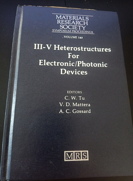
III-V heterostructures for electronic/photo
Type doc. :
Langue :
Auteur(s) :
Editeur(s) :
Année d'édition :
Thème :
ISBN :
Afficher le Résumé
III–V semiconductors (such as GaAs, InP, InGaAs, etc.) enable the formation of heterostructures — stacks of different material layers with distinct energy bands, lattice constants, or optical properties — allowing precise control over electronic and optical characteristics in devices. In the electronic domain, these heterostructures make it possible to create high-mobility channels, well-defined potential barriers, and quantum wells, which enhance the performance of transistors, diodes, integrated lasers, and other components. In photonic or photo-electronic applications, III–V heterostructures play a major role: they allow fine-tuning of the band gap and band alignment to optimize light absorption, emission, or photoelectric conversion (e.g., solar cells, photodetectors, optical sources). Moreover, heterogeneous integration (for example, combining III–V materials with silicon) and structures such as quantum wells, quantum dots, or nanowires open new possibilities for compact, multifunctional, high-density devices III–V semiconductors (such as GaAs, InP, InGaAs, etc.) enable the formation of heterostructures — stacks of different material layers with distinct energy bands, lattice constants, or optical properties — allowing precise control over electronic and optical characteristics in devices. In the electronic domain, these heterostructures make it possible to create high-mobility channels, well-defined potential barriers, and quantum wells, which enhance the performance of transistors, diodes, integrated lasers, and other components. In photonic or photo-electronic applications, III–V heterostructures play a major role: they allow fine-tuning of the band gap and band alignment to optimize light absorption, emission, or photoelectric conversion (e.g., solar cells, photodetectors, optical sources). Moreover, heterogeneous integration (for example, combining III–V materials with silicon) and structures such as quantum wells, quantum dots, or nanowires open new possibilities for compact, multifunctional, high-density devices
| N° Bulletin | Date / Année de parution | Titre N° Spécial | Sommaire |
|---|
| N° d'Exemplaire / inventaire | Cote | Localisation | Type de Support | Type de Prêt | Statut | Date de Restitution Prévue | Réservation |
|---|---|---|---|---|---|---|---|
| 111599A92 | 621.381 MAT 4 C1 | BIB-Centrale / Ouvrages | Papier | interne | disponible | ||
| 111600A92 | 621.381 MAT 4 C2 | BIB-Centrale / Ouvrages | Papier | interne | disponible |